Bm5291 Ver 13 Schematic Free ^hot^
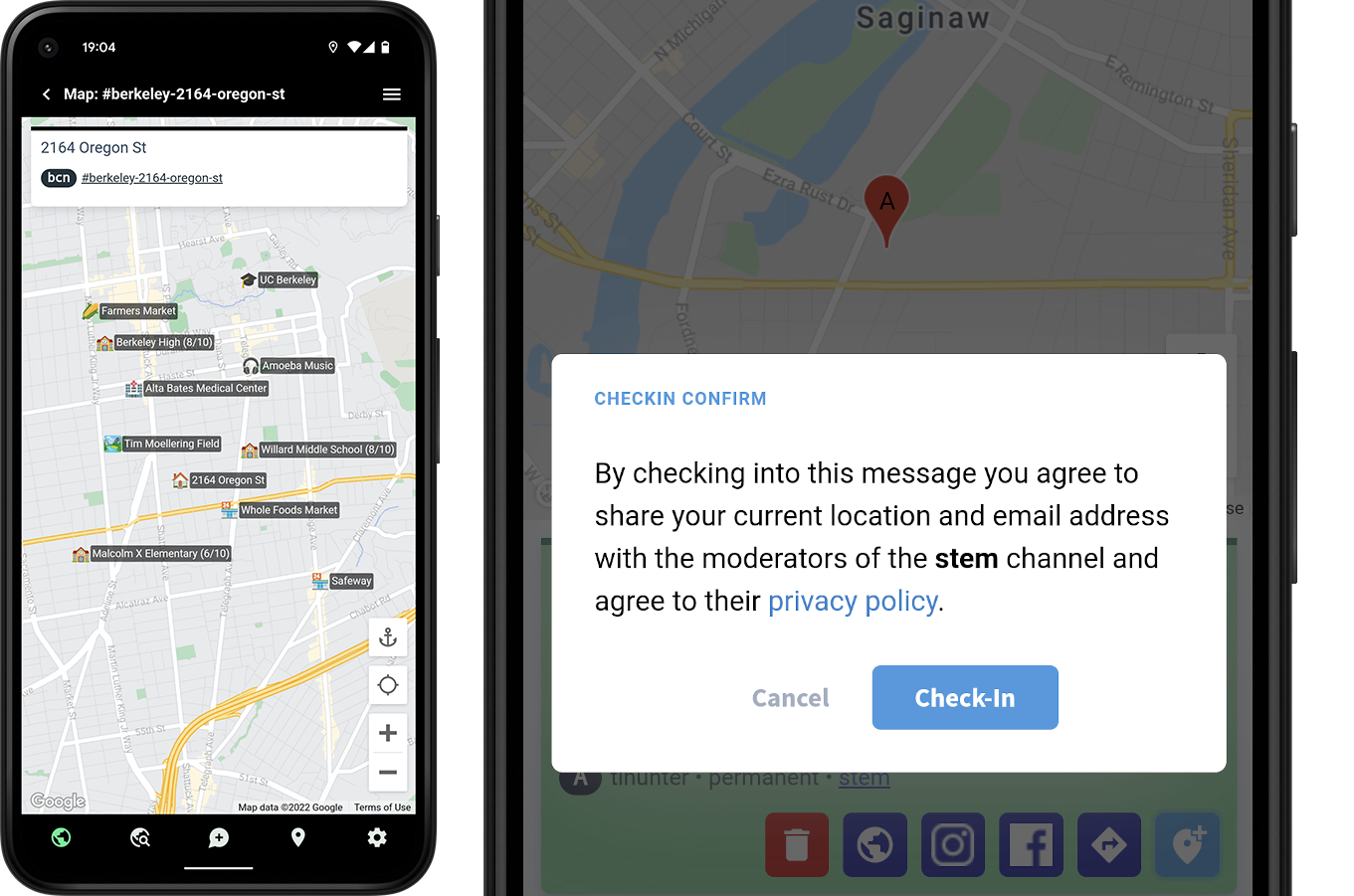
Discover, subscribe, and create interactive maps.


Discover, subscribe, and create interactive maps.
Leave a post somewhere in the world and others can only find it if they visit the same location.
Posts are organized into maps. Subscribe to maps that interest you, like foodtrucks, coffee, or garage-sales.
Choose how “loud” your posts are, whether it be a long-lived whisper or a short-lived shout.
If you cannot find a downloadable PDF layout for Version 13, you can map out the circuit using these reverse-engineering strategies:
While manufacturers do not typically release these diagrams to the public, the technical community often shares them for repair purposes. A standard BM5291 schematic includes:
Working with multi-cell lithium battery packs carries inherent risks. Always follow these safety protocols:
Small surface-mount resistors labeled with values like "680" or "101," used for balancing. Where to Find the Schematic/Manual bm5291 ver 13 schematic free
When troubleshooting the BM5291 Ver 13, you can use the voltage markers printed directly on the PCB silkscreen as a "mini-schematic." The primary output connector linking the power board to the main logic board typically utilizes the following pin configuration: Expected Voltage (Standby) Expected Voltage (Active) Description Standby power for the microprocessor PS_ON 3.3 V – 5.0 V Trigger signal from main board to switch on power GND Ground reference 12V Powers audio chips and signal processors 24V Feeds the LED backlight driver circuit BL_ON Backlight On/Off control signal PWM/DIM 1.0 V – 3.3 V Pulse Width Modulation for brightness dimming Common Failure Modes on the BM5291 Ver 13
If you cannot find the digital file, you can create your own reference. The BM5291 is usually a 4-layer or 2-layer board.
Ensure your soldering iron tip is isolated and use ceramic or insulated tweezers when probing components. If you cannot find a downloadable PDF layout
Rectify the high-frequency AC coming out of the transformer back into smooth DC.
This comprehensive guide covers how to safely locate this schematic, understand the board's architecture, and troubleshoot common circuit failures. 1. Understanding the BM5291 Ver 13 Board
Searching for free schematics online can be a minefield. Many websites promising a "free download" are actually: Where to Find the Schematic/Manual When troubleshooting the
Tracing clock signals or keyboard and touch interface lines for diagnostic purposes. Where to Find Free Schematics
Activating internal bypass resistors when a specific cell exceeds the balancing threshold (typically 4.2V). The Control Logic & MOSFET Gate Drives
Familiarize yourself with how 74-series ICs and EPROMs are mapped in the circuit to assist in troubleshooting. Conclusion
Finding these documents for free can be tricky, as they are often hosted on specialized technician forums or shared via community archives. Below is a guide on where to find the schematic, what it covers, and how to use it for common repairs. Where to Find the BM5291 Ver 13 Schematic Free
Locate the small PWM IC on the primary side and the Boost IC on the LED driver side. Write down their part numbers (e.g., OB2273, LD7536, or similar industry standards).
If you cannot find a downloadable PDF layout for Version 13, you can map out the circuit using these reverse-engineering strategies:
While manufacturers do not typically release these diagrams to the public, the technical community often shares them for repair purposes. A standard BM5291 schematic includes:
Working with multi-cell lithium battery packs carries inherent risks. Always follow these safety protocols:
Small surface-mount resistors labeled with values like "680" or "101," used for balancing. Where to Find the Schematic/Manual
When troubleshooting the BM5291 Ver 13, you can use the voltage markers printed directly on the PCB silkscreen as a "mini-schematic." The primary output connector linking the power board to the main logic board typically utilizes the following pin configuration: Expected Voltage (Standby) Expected Voltage (Active) Description Standby power for the microprocessor PS_ON 3.3 V – 5.0 V Trigger signal from main board to switch on power GND Ground reference 12V Powers audio chips and signal processors 24V Feeds the LED backlight driver circuit BL_ON Backlight On/Off control signal PWM/DIM 1.0 V – 3.3 V Pulse Width Modulation for brightness dimming Common Failure Modes on the BM5291 Ver 13
If you cannot find the digital file, you can create your own reference. The BM5291 is usually a 4-layer or 2-layer board.
Ensure your soldering iron tip is isolated and use ceramic or insulated tweezers when probing components.
Rectify the high-frequency AC coming out of the transformer back into smooth DC.
This comprehensive guide covers how to safely locate this schematic, understand the board's architecture, and troubleshoot common circuit failures. 1. Understanding the BM5291 Ver 13 Board
Searching for free schematics online can be a minefield. Many websites promising a "free download" are actually:
Tracing clock signals or keyboard and touch interface lines for diagnostic purposes. Where to Find Free Schematics
Activating internal bypass resistors when a specific cell exceeds the balancing threshold (typically 4.2V). The Control Logic & MOSFET Gate Drives
Familiarize yourself with how 74-series ICs and EPROMs are mapped in the circuit to assist in troubleshooting. Conclusion
Finding these documents for free can be tricky, as they are often hosted on specialized technician forums or shared via community archives. Below is a guide on where to find the schematic, what it covers, and how to use it for common repairs. Where to Find the BM5291 Ver 13 Schematic Free
Locate the small PWM IC on the primary side and the Boost IC on the LED driver side. Write down their part numbers (e.g., OB2273, LD7536, or similar industry standards).
Map Buddy aims to be the one-stop application for finding any information that is both time and location sensitive. Reserve your username and map while they're still available!
Try Map Buddy for Web